The Sanctions Paradox: Huawei's Impossible Challenge
The central enigma is Huawei. Blacklisted by the US and barred from ASML's essential EUV lithography, how can it develop a processor to challenge Nvidia?
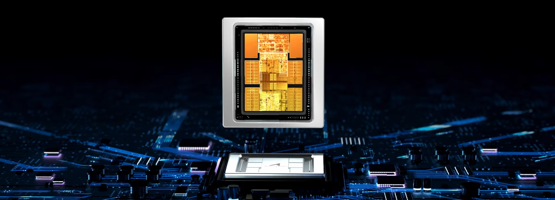
Nvidia's H100 and its successors rely on TSMC's most advanced 4nm and 3nm nodes. Without access to this technology, conventional wisdom dictates Huawei is fundamentally locked out of the high-end AI chip race. For industry experts, the blacklisted giant is attempting the impossible.
The Reveal: Patent WO2024222427A1
Huawei's path forward is not a frontal assault on process nodes. The company is executing a flanking maneuver, detailed in patent application WO2024222427A1. This blueprint bypasses the lithography barrier by fundamentally changing the game with advanced packaging.
Deconstructing the Strategy: Chiplets Over Monoliths
A Blueprint for Scale: The Quad-Chiplet Design
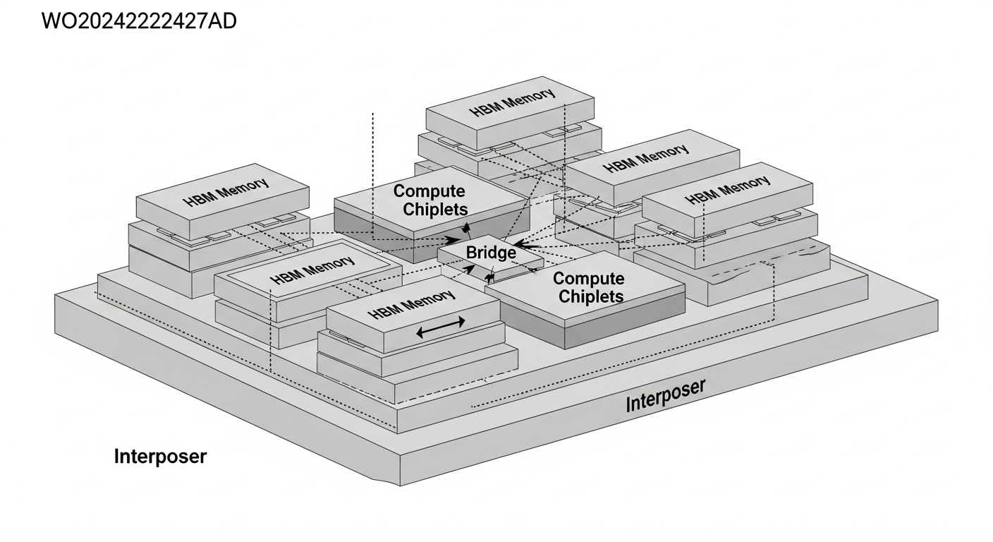
The patent details a quad-chiplet design, reportedly for the Ascend 910D AI accelerator. Huawei plans to connect four less-advanced chiplets—likely from SMIC's 7nm or 5nm-class nodes—on a 'smart' interposer. These chiplets are linked by high-density interconnections, or 'bridges,' akin to TSMC’s CoWoS-L or Intel’s EMIB. This method aggregates the performance of smaller dies to create a single, powerful processor package designed to rival monolithic Nvidia GPUs. The packaging-centric approach achieves massive scale, with a speculative total silicon area exceeding 4,000 mm².
The New Battlefield: Packaging Is the New Process Node
The Packaging Arms Race
Geopolitical pressure is forcing advanced packaging from a manufacturing footnote into a primary vector of competition. Analysis indicates Huawei is developing packaging techniques to rival market-leader TSMC, creating a viable route to bypass US sanctions on leading-edge fabrication. The ambition is clear: its rumored design requires a packaging scale—five EUV reticle sizes—that TSMC only plans for volume production in 2026.
Innovation Forged by Geopolitical Fire
US sanctions, intended to halt Huawei, have instead catalyzed a radical, asymmetric innovation. The AI hardware race is no longer defined solely by access to the most advanced lithography. It is now a multi-front conflict where ingenuity in chiplet architecture and advanced packaging can challenge raw manufacturing might. Huawei's strategy, as outlined in its patent, signals the official opening of this new competitive front in the global technology war.
